Are you looking for a specific wafer-level or assembly process, or do you want to develop one? From simple thin-film deposition on a wafer substrate to full device development for a sensor, G3C connects you with the infrastructure of the APECS pilot line and other European pilot lines, as well as competent development teams to implement your idea.
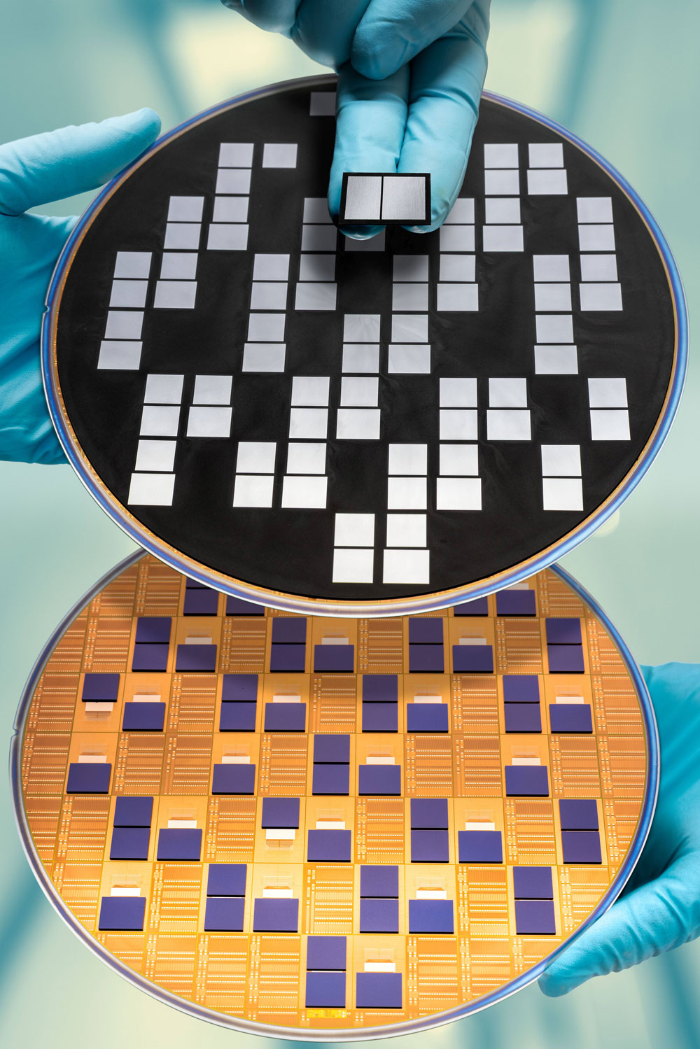
A key focus of the German APECS pilot line is heterogeneous integration—for example, chiplets, stacked wafers, or direct (quasi-monolithic) integration on existing CMOS wafers. We connect you with service providers and provide access to tools and equipment for various packaging and assembly techniques, and we pre-screen your idea for an initial feasibility assessment.
Contact us! The G3C team will get back to you and guide you through the next steps.